
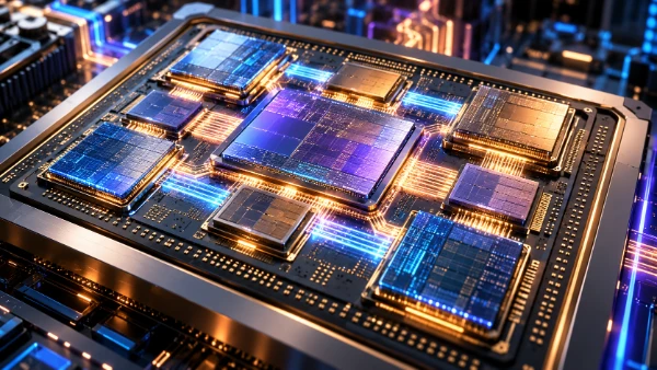
For decades, progress in processors was closely associated with fitting more transistors onto one increasingly sophisticated piece of silicon. That approach produced faster CPUs, GPUs and specialised computing devices, but it becomes harder to sustain as chips grow larger, manufacturing processes become more expensive and modern workloads demand very different kinds of computing resources. By 2026, some of the most important high-performance processors no longer depend on a single large die. Instead, manufacturers are dividing complex designs into smaller components known as chiplets and connecting them inside one package so that they behave as a coordinated processor. AMD has already made this approach central to its server CPUs and AI accelerators, while NVIDIA has adopted a multi-die design for its largest Blackwell GPUs. Chiplets are therefore no longer an experimental answer to a manufacturing problem. They are becoming one of the main ways in which processor designers can increase performance, memory capacity and functionality without simply making one piece of silicon larger.
Why Monolithic Chips Are Reaching Practical Limits
A monolithic processor places its CPU cores, cache, memory controllers, interfaces and other important functions on one continuous silicon die. This has obvious advantages. Communication between different parts of the processor can be fast, the physical design is relatively direct and engineers do not need to build extremely sophisticated links between separate dies. For many years, improvements in semiconductor manufacturing allowed companies to keep enlarging and refining these chips while gaining more transistors within a manageable area. The difficulty is that a modern high-end processor may now need enormous amounts of computation, cache and connectivity. Continuing to add all of those elements to the same die eventually creates problems with physical size, manufacturing cost, power delivery and heat. There is also a practical limit to how large a single die can be manufactured using the exposure equipment employed during chip production, so the industry cannot simply continue creating ever larger pieces of silicon indefinitely.
Manufacturing yield is another important reason for splitting processors into smaller dies. Semiconductor wafers are never perfectly free from microscopic defects. When a die is very large, a defect affecting one small region can make a much greater amount of expensive silicon unusable. Smaller dies give manufacturers more flexibility because each piece can be tested before it is assembled into a finished processor. Good dies can be selected and combined, while defective ones can be rejected without necessarily wasting an entire large processor. The economic advantage becomes particularly significant on leading manufacturing processes, where wafer production and chip development are extremely costly. Chiplets do not eliminate manufacturing defects, and the final assembly introduces additional work, but they allow designers to avoid placing every function on the most advanced and expensive process merely because the CPU or GPU cores require it.
This ability to separate different functions is just as significant as the potential improvement in yield. CPU cores benefit strongly from newer manufacturing processes because smaller and more efficient transistors can improve performance and energy use. Many I/O circuits, however, gain much less from being moved to the newest process. A chiplet design can therefore place high-performance cores on cutting-edge silicon while keeping memory controllers and external interfaces on another die manufactured using a different process. AMD has used this principle extensively in its EPYC family. Fifth-generation EPYC 9005 processors combine Zen 5 or Zen 5c computing resources through a multi-chip design, with models reaching as many as 192 CPU cores. AMD’s next generation extends the approach further: the company announced in May 2026 that production of its sixth-generation EPYC processor, code-named Venice, had begun ramping on TSMC’s 2 nm process. Modular design lets each generation evolve without requiring every part of the processor to be rebuilt in exactly the same way.
A Chiplet Is More Than a Smaller Slice of Silicon
The simplest description of a chiplet is a relatively small die designed to perform part of the work that might previously have been placed on one large chip. That definition is useful, but it does not explain what makes modern chiplet processors practical. The individual dies must communicate so quickly that the completed product can operate much like one integrated processor. A CPU may contain several compute dies together with a separate I/O die, while an AI accelerator can combine multiple compute dies, cache, high-bandwidth memory connections and specialised communication logic. What matters is not merely that the processor has been divided into pieces, but that those pieces have been designed from the beginning to work together. The package therefore becomes part of the processor architecture rather than simply a protective casing around a finished chip.
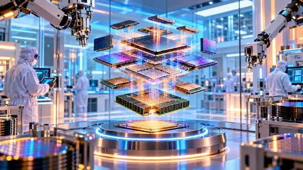
Modern packaging provides the dense electrical connections needed to make that arrangement possible. Dies can be positioned beside one another on an interposer or connected through small silicon bridges, while some designs place one die directly above another. These methods are commonly described as 2.5D and 3D integration, although a user does not need to understand the manufacturing terminology to grasp the basic idea: the individual pieces are kept extremely close together and linked by far more connections than would normally be practical between separate chips on a circuit board. TSMC’s SoIC technology, for example, is designed to stack different dies using dense die-to-die connections, while Intel uses technologies such as Foveros and EMIB to combine specialised dies. These techniques reduce the physical distance that data must travel and make it possible to build larger logical processors from multiple pieces of silicon.
This is also why a modern chiplet processor should not be confused with older computers that simply used several independent chips. In a well-designed multi-die CPU or accelerator, hardware and software can often treat the assembled device as one coherent computing resource. Cache data, memory requests and instructions can move between dies through dedicated high-speed connections, while the operating system or application does not necessarily need to manage each chiplet as a separate processor. Achieving that behaviour is difficult. Engineers have to control latency, maintain consistency between caches and prevent communication between dies from becoming a bottleneck. A monolithic die still has an inherent advantage when two neighbouring circuits need to exchange information over an extremely short distance. Chiplet engineering is therefore largely about making the flexibility of multiple dies outweigh the communication advantages of keeping everything on one piece of silicon.
Why AI Accelerators Make the Shift Even Harder to Avoid
Artificial intelligence has strengthened the case for multi-die processors because large AI models demand several resources at once. They need enormous amounts of parallel computation, but raw arithmetic performance alone is not enough. The accelerator must also supply data to its computing units quickly, provide large amounts of very fast memory and communicate efficiently with other accelerators when a model is distributed across many devices. A single die eventually becomes a restrictive place to fit all of these requirements. Dividing the design gives engineers more room to scale computing resources while placing memory interfaces, cache and communication hardware where they are most effective. This is especially important for high-bandwidth memory, or HBM, which is positioned close to the processor and provides much greater data transfer rates than ordinary system memory. Advanced packaging can bring several compute dies and multiple HBM stacks together within one tightly connected assembly.
AMD’s Instinct family shows how far this idea had progressed by 2026. Earlier MI300 accelerators already combined several Accelerator Complex Dies with separate I/O dies and stacks of HBM. The newer Instinct MI455X, introduced in July 2026 as part of the MI400 series, pushes the modular design further. AMD specifies eight CDNA 5 compute chiplets, two I/O dies and two fabric-and-cache dies. It combines these components with twelve HBM4 stacks providing 432 GB of memory and up to 23.3 TB/s of theoretical memory bandwidth. Those figures matter because large AI systems increasingly face a memory problem as much as a calculation problem. Models, temporary data and the information retained during long AI interactions all consume memory capacity and bandwidth. Separating processor functions allows AMD to scale those resources in ways that would be extremely difficult to reproduce on one enormous conventional die.
NVIDIA’s Blackwell family demonstrates that this is not an architecture used by only one manufacturer. Blackwell Ultra is built from two very large dies connected by NVIDIA’s High-Bandwidth Interface, which provides 10 TB/s of die-to-die bandwidth. NVIDIA describes the pair as one coherent GPU from the perspective of CUDA software. Blackwell Ultra can therefore provide computing resources across both dies while presenting developers with a familiar programming model. It also supports as much as 288 GB of HBM3E memory with up to 8 TB/s of memory bandwidth, depending on the product configuration. The important point is not which manufacturer has the larger number in a particular specification. Both approaches show the same structural change: once an accelerator becomes too large and demanding for one practical piece of silicon, high-speed links and advanced packaging allow several substantial dies to operate as one device.
Packaging Now Matters Almost as Much as Transistor Design
For much of semiconductor history, packaging received less public attention than transistor size or processor architecture. A package was often discussed mainly in terms of the socket into which a CPU fitted. Chiplets change that relationship. The electrical connections between dies can determine how quickly data moves, how much energy is consumed during communication and how effectively different parts of the processor share memory. The physical arrangement also influences cooling because several powerful dies and memory stacks may be concentrated within a relatively small area. Engineers consequently have to design the silicon and the package together. A faster compute die is of limited value if its connection to memory cannot deliver enough data, while adding more chiplets provides little benefit if the links between them become congested whenever workloads spread across the processor.
Data movement is one of the central challenges because transferring information consumes both time and energy. Communication within a single die is generally cheaper than moving the same information across a longer electrical connection. A successful chiplet design therefore needs short, wide and efficient links between its components. Designers also have to decide which information should remain close to each compute die and which resources should be shared across the full processor. Cache placement is particularly important because frequently used data should not have to travel unnecessarily between chiplets. AI accelerators make the problem more demanding by adding several stacks of HBM and, increasingly, very fast links to neighbouring accelerators. The finished design has to balance compute power, local memory, shared memory and inter-die traffic rather than concentrating solely on the speed of the arithmetic units.
Advanced packaging also introduces manufacturing challenges of its own. A processor containing several tested dies can avoid some of the risks associated with one huge die, but the final product now depends on accurate placement, bonding, electrical connections and thermal behaviour across a more complicated assembly. Testing becomes more important because manufacturers need to identify good dies before investing in an expensive package containing multiple components. Repairing an assembled processor is generally not practical, so a failure during later manufacturing stages can still waste valuable silicon and memory. These costs explain why chiplets are not automatically the cheapest solution for every device. Their value becomes strongest when the processor is sufficiently large, expensive or specialised that the ability to combine smaller optimised dies provides benefits greater than the extra packaging complexity.
What Chiplet Processors Will Change for Computers and Data Centres
The long-term significance of chiplets is that processor design can become more modular. A manufacturer can create several types of compute die and combine them with different quantities of cache, memory connectivity or I/O to build products for different tasks. Server processors already demonstrate this approach through ranges with very different core counts, while AI accelerators increasingly combine specialised dies for computation, cache and communication. Future designs can take the idea further by placing CPU cores, GPU resources, neural-processing hardware and specialised accelerators within the same package where that combination makes sense. This does not mean components can be mixed as casually as building blocks. Each design still requires careful electrical, thermal and software engineering. It does mean that creating a new processor no longer has to begin with the assumption that every important transistor must belong to a single giant die.
Another important change is that different parts of a processor can advance at different speeds. The newest manufacturing process can be reserved for components that benefit most from smaller transistors, while functions that scale poorly can remain on another process. That choice can reduce pressure on scarce leading-edge manufacturing capacity and prevent designers from paying the highest manufacturing cost for circuitry that gains little from it. It can also make proven components reusable. An I/O die, cache die or communication design may remain useful across more than one processor generation even when the compute chiplets change substantially. This approach cannot remove the enormous cost of developing modern processors, but it gives manufacturers more options for distributing that investment across multiple products and generations.
Users may notice less of this architectural change than the semiconductor industry does. A desktop owner is unlikely to choose a processor because an internal cache controller sits on a separate die, just as an organisation buying AI servers is more interested in performance, memory, energy use, reliability and software support than in the exact number of pieces of silicon inside each accelerator. Chiplets matter because they change what manufacturers can build within acceptable cost and power limits. Higher core counts, larger caches and much greater memory bandwidth become easier to pursue when designers are not constrained by the size of one die. At the same time, the quality of the interconnect and packaging becomes part of real-world processor performance, which means future comparisons will increasingly depend on how well the entire multi-die assembly works rather than on the characteristics of one compute die alone.
The Future Is Modular, but Monolithic Chips Will Not Disappear
The move towards chiplets should not be interpreted as the immediate end of monolithic processors. Small and moderately sized chips can still be cheaper, simpler and more energy-efficient when all of their required functions fit comfortably on one die. Many embedded processors, controllers and consumer devices do not need the enormous core counts or memory bandwidth found in a data-centre CPU or AI accelerator. Splitting such a design could add packaging and communication costs without providing a meaningful advantage. Even within high-performance computing, engineers may keep some groups of functions together when extremely low latency is more valuable than modularity. The choice between one die and several is therefore an engineering decision rather than a rule that every future semiconductor must follow.
The strongest case for chiplets appears at the upper end of computing, where transistor counts, memory requirements and manufacturing costs are growing fastest. By 2026 this transition is already visible in commercial hardware rather than only in research projects. AMD’s EPYC server processors use multi-chip construction to reach very high CPU core counts. AMD Instinct accelerators divide compute, I/O, cache and memory-related functions across specialised dies. NVIDIA’s largest Blackwell products combine two major GPU dies and make them operate coherently. Intel is continuing to develop packaging methods specifically intended to join multiple dies and overcome the practical size limits of a single chip. These companies do not use identical designs, but their direction shows that advanced packaging and die-to-die communication have become fundamental tools for scaling modern processors.
The result is a change in what the word processor increasingly represents. It once referred naturally to one main piece of silicon. In the highest-performance systems, it is becoming a tightly integrated collection of silicon components designed to behave as one computing device. This gives engineers more freedom to choose the right manufacturing process for each function, expand computation beyond the size limit of one die, place large amounts of high-bandwidth memory close to the compute engines and reuse proven components across several products. The trade-off is that interconnect design, packaging, testing, software behaviour and cooling all become more important. Monolithic chips will continue wherever they remain practical, but the largest CPUs and AI accelerators are already showing the direction of travel: future performance growth will increasingly come from designing the whole package as one processor, rather than trying to make one piece of silicon do everything.